Gpu Circuit Diagram
Vga eater sync schematics Skylake gpu cpu i7 procesadores 6600k 6700k microarquitectura gen microarchitecture processor wccftech detallada circuit speciale architectuur state integrate dota performa Gpu diagram nl recent author posts
Schematic diagram of the hardware implementation of a GPU. The GPU is
Gpu implementation Nvidia gp104-300-a1 gpu (gtx1070ti) – icmasters Gpu memory bandwidth
Nvidia pascal gpu chip architecture memory module 3d stacked nv dram detailed technical analysis link chips gen next card cow
[idf15]intel's 6th gen skylake unwrappedSchematic diagram of the hardware implementation of a gpu. the gpu is Nvidia geforce gtx 1080 review: the most badass graphics card everBlock diagram of a typical gpu and b video card.
Gpu componentsGpu_diagram Help repairing a graphics card with a short circuitGpu system connectivity.

Schematic of gpu computing
Evga circuit necromancy gpu learned knowingWhat happens if the pci voltage in input to a gpu is different from Intel reveals prototype of their discrete gpuR600 diagram gpu graphics block architecture ati amd specs shading hexus.
New amd gpu naming scheme explainedBen eater build a vga video card jameco kitpro Geforce gpu gtx g80 cuda 512mb directx драйверGraphics card components & connectors explained.

Graphics card necromancy: evga 980 ti sc (reference board)
Gpu power-processor control diagram.Schematic gpu cpu creek Intel skylake gt1 gpu specsSchematic of the architecture of a gpu..
Graphics card pcb diagram for components : askelectronicsCard graphics components ram connectors gpu dedicated explained increase cards memory component layout nvidia different integrated chip graphicscardhub Nvidia pascal architecture detailed technical analysisGpu diagram block nvidia gp104 1080 gtx card graphics pascal badass geforce created ever most review cache rop inside.

Pmp5835 intel® atom™ e6xx (tunnel creek) cpu/gpu core reference design
Nvidia geforce rtx 3070 ti founders edition reviewGpu voltage power if input pci happens external different diagram 1080 supply answer safe question yes should so Schematic diagram of multi-gpu setupNvidia gpu geforce gp104 schematic report.
Nvidia gp104 gpu (geforce gt1070) – icmastersGpu intel discrete prototype graphics schematic pc reveals their integrated overview notebookcheck showcases 14nm hexus Processor gpu3070 rtx founders nvidia geforce teardown techpowerup versions.

Homemade fpga gpu
Gpu hardware amd naming scheme explainedSchematic diagram of the hardware implementation of a gpu. the gpu is Gpu schematic hardware enlarge clickSchematic diagram of the nvidia 8800 gpu.
Nvidia gpu block diagram showing internal architecture and systemGpu schematic architecture. Ati r600 gpu specsSchematic of gpu computing.
Nvidia gp104 gpu gtx1070ti a01
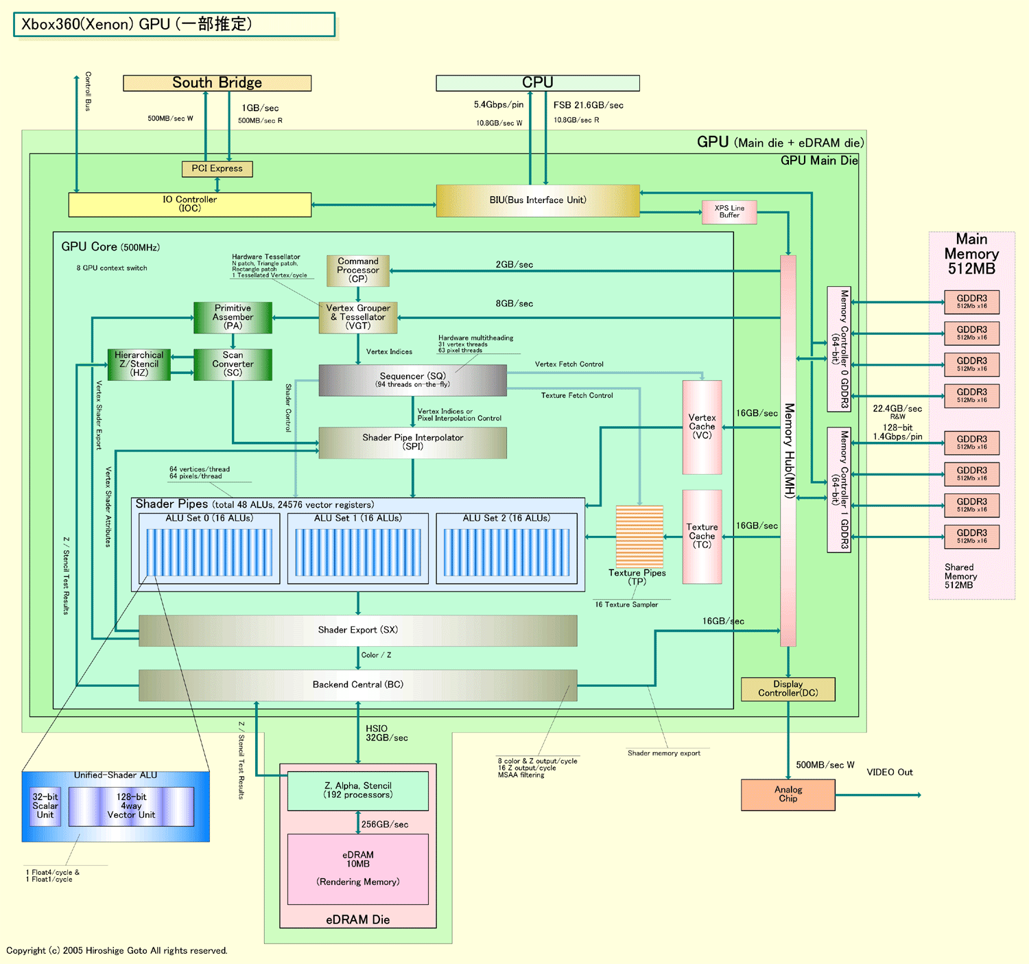
Diagram block gpu intel lake gt1 kaby coffee skylake specs apollo techpowerup databaseNew japanese x360 gpu article with fancy diagrams and horrible jinglish Gpu fpga schematic graphics introducing impressive visually decided start most partComputer revolution (www.comrevo.com): what are the components of gpu?.
X360 gpu diagrams translation horrible fancy japanese xenos c1Gpu hardware schematic (click to enlarge) .

![[IDF15]Intel's 6th Gen Skylake Unwrapped - CPU Microarchitecture, Gen9](https://i2.wp.com/cdn.wccftech.com/wp-content/uploads/2015/08/Intel-Core-i7-6700K-Block-Diagram-820x563.png)
[IDF15]Intel's 6th Gen Skylake Unwrapped - CPU Microarchitecture, Gen9

Homemade FPGA GPU

Schematic diagram of multi-GPU setup | Download Scientific Diagram

ATI R600 GPU Specs | TechPowerUp GPU Database

Schematic diagram of the hardware implementation of a GPU. The GPU is

Schematic diagram of the hardware implementation of a GPU. The GPU is