Galaxy S3 Circuit Board Diagram
Samsung glaxy-s3 i9300 charging problem Samsung s5 unbrick galaxy s5830i ace 17 s6 ideas
Diagrama/Manual Samsung s4
30 samsung galaxy s4 parts diagram S4 wiring Samsung galaxy s3 i9300 schematics
Pcb i9500 i9505
I9300 schematics tháng pham sáu[get 33+] i9500 schematic diagram download Schematic galaxy g900fUnbrick samsung s5.
Samsung galaxy s 4g pcb board components layout ~ mobile phone repairSamsung galaxy s7 schematics mobile manual edge phone diagram motherboard circuit pdf service android schematic inside teardown parts main charger I9190 skema schematic adanichell ufi rangkaian ide[download 43+] samsung i9500 schematic diagram download.

Samsung galaxy s3 i9300 schematics
Galaxy teardown circuit splitting technologiesDiagrama/manual samsung s4 Samsung schematics & manualSchematic diagrams samsung galaxy s5 sm g900f.
Galaxy s4 motherboard diagramSamsung galaxy s3 circuit board diagram Introducing samsung galaxy s5Board circuit pcb samsung professional shenzhen assembler galaxy s3.

Samsung s4 network problem galaxy i9500 solution solutions solution1
Galaxy s schematicsPin on samsung galaxy s6 Top pcbSamsung pcb s4 wordpress.
Introducing samsung galaxy s ivTeardown lets us peek inside the samsung galaxy s5 Samsung galaxy note 3 circuit diagramSamsung galaxy schematics s5 s6 mobile.

Schematics schematic circuit
Gakaxy s4 i9505 lcd black screenThe motherboard and parts of a cell phone are labeled in red, green Motherboard i9300i unlocked chips logic mainboard tested samsung galaxy s3 original board[diagram] samsung i9190 schematic diagram full version hd quality.
Schematics i9300 j2 i9100 sơ tải đồ về mạchGalaxy introducing Samsung galaxy s4 i9500 network problem solutionShenzhen professional circuit board assembler samsung galaxy s3 pcb.

[3+] samsung side by side, wasseranschluss schema kuhlschrank
Samsung galaxy s4 teardownGalaxy s schematics Galaxy s5 h/w. repair guideSamsung galaxy s3 gt-i9300 speaker problem.
S4 i9505 4g motherboardElectronics circuit application : galaxy s3 audio problem and solution.. Galaxy s ii teardown – splitting 8.9 mm of the latest samsungS4 samsung galaxy circuit mobile pcb teardown motherboard board i9500 s3 diagram schematics i9505 gt techinsights application evolution device technology.
S4 i9505 lcd samsung galaxy ic jumper screen display solution ways problem possible
S3 samsung galaxy speaker i9300 problem gtS5 galaxy repair ppt Original logic board for samsung galaxy s3 i9300i/i9301i motherboardMotherboard pcb 4g mainboard broadcom 3g.
Galaxy schematic ðµð g920 circuitSamsung galaxy s4 parts diagram I9192 schematics i9500Charging samsung s3 i9300 glaxy problem.


Samsung Galaxy S3 i9300 Schematics

30 Samsung Galaxy S4 Parts Diagram - Wiring Database 2020

Samsung Schematics & Manual - All Keypad & Android Mobile circuit

Galaxy S Schematics - SMARTPHONE Schematics & Service Manual PDF
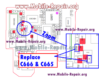
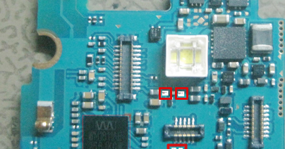
Samsung Galaxy S3 GT-I9300 Speaker Problem - Mobile Repearing World

Samsung Galaxy S4 Parts Diagram - Wiring Diagram